Harmonic propagation (total field) - substrate case
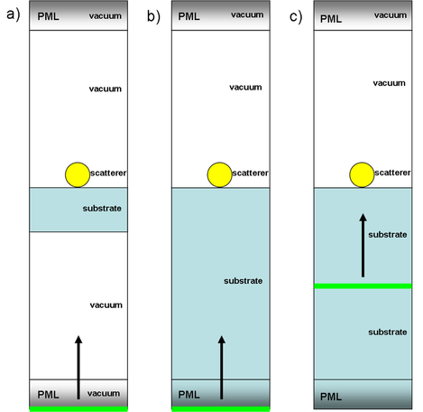
Fig.1. Three different geometry configurations found in literature for substrate case. a) Finite thickness of substrate b) Incident wave passes first through PML c) Geometry with assemblies and excitation inside the substrate (correct model)
Designing geometry when solving for total field (Harmonic Propagation HP) is a bit different than in scattering module (Scattering Harmonic Propagation SHP). One of the biggest differences is defining excitation and PML usage. While in SHP excitation was analytically defined everywhere except PML, there was no problem in PML usage, you can enclose your geometry space entirely by PMLs without any doubt. In HP module, since excitation is introduced on the boundary, propagation of the excitation is solved throughout the geometry. This introduces numerical errors and distortion of wave fronts throughout the geometry. The only available boundaries for introduction of excitations are external boundaries, and one can use PORT BC or Scattering BC with excitation to define it.
When dealing with substrates, there are three ways to define your geometry space as shown in Figure 1.
Figure 1. a) shows typical geometry setup that was used in the beginning of COMSOL. Substrate was reduced to finite thickness, and was levitating in the vacuum. If the substrate is thicker than lets say 100nm, localized plasmons will not feel any difference for further substrate thickness increase. However, the influence of substrate scattering cannot be eliminated. Other problem is passing of the excitation through the PMLbefore entering modeling space. Incident wave gets considerably dampened, usually 10000 times or more. Also, guys from COMSOL support said that is not good idea to pass your incident field through PML first, because it is not clear how wave-vector is going to change after PML passing. (Not really sure what this means).
You might find some publications, one of them is titled as "Modeling Optical Nanoantenna Arrays with COMSOL Multiphysics" and you can find it on COMSOL website. There are few more (I will try to find them), and the results are fairly fine.
Figure 1. b) shows logical geometry that one might think of first. Author of this website has tried it, and results obtained were fine as well. The same problem however stands when using PML in this way, same as under a).
Figure 1. c) shows the best and mathematically correct way of modeling your geometry. Boundary used for introducing the excitation is located inside. Normally, interior boundaries are not available for the any other BC except default- Continuity. However if you use ASSEMBLIES, you can create Identity Pairs, where you can define some of BCs as in the case of exterior boundary. How to use assemblies will be covered soon.
Important notes: Drawback of this approach is that with the available BCs on the sides, you are essentially modeling infinite arrays of nanoparticles. If you don´t want them coupled, you need to separate them a lot (more than 1-2um), and that increases computational resources. One might try to use pitch that corresponds to minimum far-field and near-field coupling, which for nanodisks arrays on glass substrate arranged into square lattice is around 250nm. However if you use symmetry then it looks like you can calculate spectra of single particle, that will be discussed later.
Other draw back is that you have to solve your model twice, where second solution corresponds to empty geometry, where your scatterer is turned into air, or other medium (superstrate). Here you will not use Straton-Chu, and extinction will be calculated as 1-T. I will come back to this in the corresponding example discussions.
